What is Thin Film Pressure Sensor?
A thin-film pressure sensor is a type of pressure sensing device that utilizes a thin-film sensing element deposited on a substrate material. The sensing element is typically a thin layer of material, such as polysilicon, silicon nitride, or metal alloys, with a thickness ranging from a few nanometers to a few micrometers.
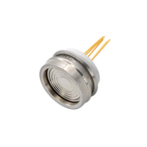
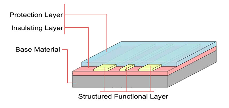
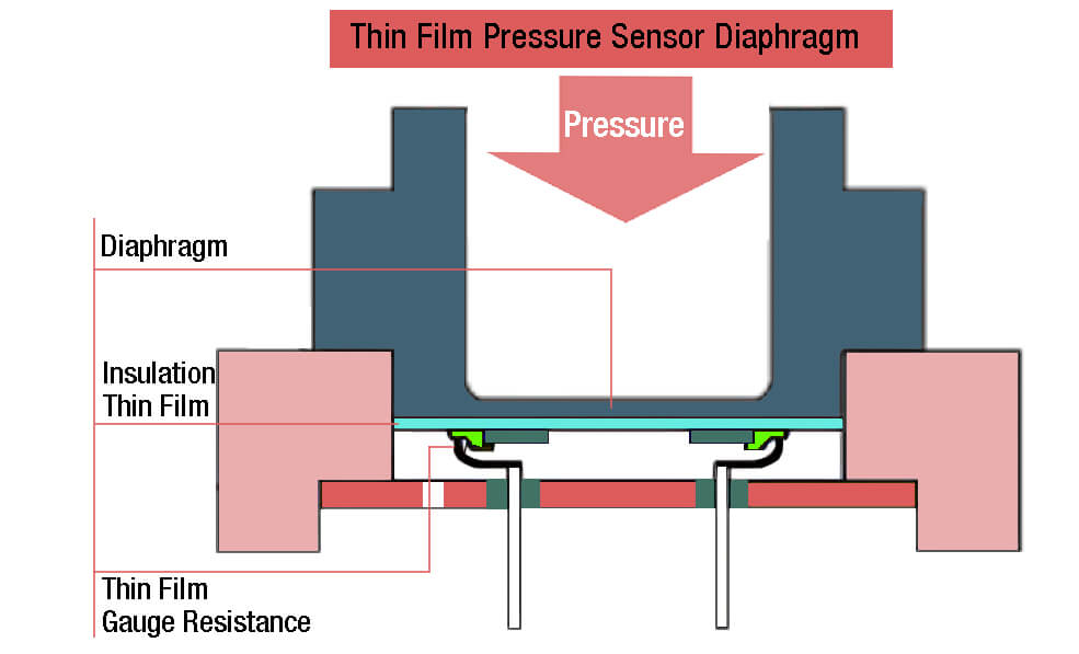
The basic structure of a thin-film pressure sensor consists of the following components:
Substrate: The substrate material serves as the base for the sensor’s construction. Common substrates used include silicon, glass, or ceramic materials.
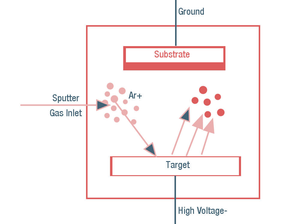
Thin-film sensing element: This is the core component responsible for pressure sensing. The sensing element is deposited on the substrate using techniques like sputtering, chemical vapor deposition (CVD), or other thin-film deposition methods.
Diaphragm: A thin, flexible diaphragm is created on the substrate, often through micromachining or etching processes. The thin-film sensing element is strategically placed on or near the diaphragm.
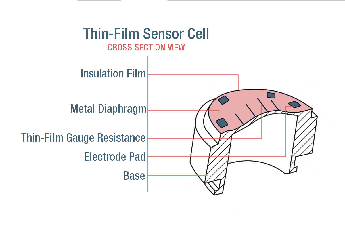
The diaphragm structure is often bonded to a backing material or a second substrate to create a sealed cavity or reference pressure chamber.
The sensing principle
The operating principle of a thin-film pressure sensor is based on the piezoresistive effect, where the electrical resistance of the thin-film sensing element changes in response to the mechanical strain or deformation caused by applied pressure.
When pressure is applied to the diaphragm, it deflects, causing the thin-film sensing element to experience strain, which in turn changes its electrical resistance.
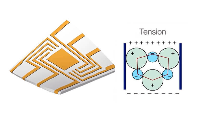
This change in resistance is detected and converted into an electrical signal using appropriate signal conditioning circuitry, allowing the measurement of pressure.
The thin-film sensing element is often configured in a Wheatstone bridge or other resistive circuit arrangement to enhance sensitivity and provide temperature compensation.
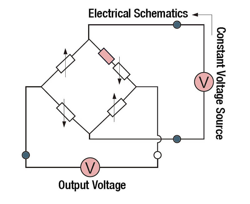
The thin-film sensing element is often configured in a Wheatstone bridge arrangement, with two active resistors (sensing pressure) and two reference resistors (not subjected to pressure). This configuration allows for temperature compensation, increased sensitivity, and common-mode noise rejection.
The change in resistance of the active resistors due to the applied pressure creates an imbalance in the Wheatstone bridge, resulting in a measurable voltage difference across the bridge’s output terminals.
The output voltage from the Wheatstone bridge is typically small and requires amplification and signal conditioning. This is achieved using instrumentation amplifiers, analog-to-digital converters (ADCs), or dedicated signal conditioning circuits.
The conditioned output signal is then processed, often by a microcontroller or digital signal processor, to calculate the corresponding pressure value. This calculation is based on the calibration data and the known relationship between the output signal and the applied pressure.
Thin-film pressure sensors can be designed and optimized for different pressure ranges, sensitivities, and environmental conditions by adjusting factors such as the diaphragm size, thickness, and material properties, as well as the dimensions and configurations of the thin-film sensing element.
Additionally, these sensors can be integrated with microelectronic circuits and signal conditioning components on the same substrate, enabling the development of compact, highly integrated pressure sensing solutions for various applications, including automotive, industrial, medical, and consumer electronics.
Highlight feature
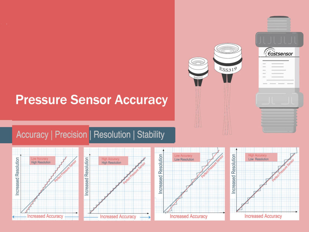
High accuracy and precision: ±0.1%-±0.25%
One of the most significant advantages of thin-film pressure sensors is their ability to achieve high accuracy and precision in pressure measurements.
High-quality thin-film sensors can typically achieve an accuracy of ±0.25% to ±0.5% of the full-scale output (FSO) or better like±0.1%.
For example, a common automotive manifold absolute pressure (MAP) sensor with a 0-5 bar range and ±0.25% FSO accuracy would have an error of ±12.5 mbar across the entire pressure range.
Wide pressure range: 0.001bar(1mbar)~2000bar
Thin-film pressure sensors can be designed to measure pressures ranging from a few millibars (mbar) to hundreds of bars, making them suitable for a wide range of applications.
For instance, some thin-film sensors can measure low pressures as low as 1 mbar, materials like sputtered or implanted polysilicon are commonly used due to their high sensitivity and good performance;
For high pressures, up to 2000 bar or even higher in specialized applications, materials like silicon carbide (SiC) or specific metal alloys (e.g., platinum, nickel-chromium) may be preferred due to their high strength and stability under extreme conditions.
The sensing element design and layout can be optimized for different pressure ranges, with larger sensing resistors for low pressures and smaller resistors for high pressures.
However, after assembly process, when such sensor has been produced pressure transmitter or transducer, in order to keep full balance and ensure long term stability, the minimal measurable range will increase to 4bar about.
On the other hand, the technics of packaging and sealing also take important effect to achieve wide pressure range.
Hermetic packaging techniques, such as welding or brazing, are essential to ensure a leak-tight enclosure and prevent moisture ingress or contaminants from affecting the sensor’s performance.
For high pressures, specialized pressure ports and fittings made of high-strength materials like stainless steel or Inconel may be required to withstand the extreme pressures without leakage or deformation.
It’s important to note that achieving such a wide pressure range often results in larger sensor sizes, higher manufacturing costs, and increased complexity. Additionally, rigorous testing and qualification processes, including pressure cycling tests, burst pressure tests, and long-term stability evaluations, are essential to ensure the reliability and performance of these specialized thin-film pressure sensors.
Temperature compensation: -20℃~120℃; -20℃~150℃/200℃
The main techniques to design a thin film pressure sensor that endures high temperatures is: Choose tough materials. Design it to handle thermal expansion. Pack it up in a material that can take the heat. Use wiring that won’t melt. Add circuits that adjust the readings when it gets hot. And don’t forget to use a temperature-resistant adhesive.
It’s important to note that designing thin-film pressure sensors for high-temperature operation often involves trade-offs in terms of sensor size, cost, and complexity. Extensive testing and qualification processes, including temperature cycling tests and long-term stability evaluations, are crucial to ensure the reliability and performance of these specialized sensors.
High burst pressure performance: 3X-10X
By carefully selecting materials, optimizing diaphragm designs, implementing robust packaging techniques, and incorporating overload protection mechanisms, it is possible to develop thin-film pressure sensors with high burst pressure capabilities, ranging from 3X to even 10X the maximum rated pressure, while maintaining the desired accuracy and performance characteristics.
How to design High Temperature thin film pressure sensor
Designing thin-film pressure sensors to withstand high working temperatures up to 150°C (302°F) requires a careful selection of materials, specialized fabrication techniques, and effective temperature compensation strategies.
Substrate Material Selection
It’s true that most silicon substrates have a temperature limit of around 125°C, beyond which their properties can degrade. For some high-temperature applications up to 150°C or higher, suitable substrate materials include aluminum nitride (AlN) and silicon carbide (SiC).
AlN has a high thermal conductivity (180-200 W/m·K) and a compatible coefficient of thermal expansion (CTE) with silicon, making it a good choice for temperatures up to 300°C.
SiC has an even higher thermal conductivity (270-370 W/m·K) and can withstand temperatures up to 600°C, making it suitable for extreme high-temperature environments.
Diaphragm Material Selection
The diaphragm material should have a compatible CTE with the substrate to minimize thermally induced stress and deformation. For temperatures up to 150°C, materials like silicon nitride (Si3N4), polysilicon, or silicon carbide (SiC) can be used for the diaphragm.
Si3N4 has good mechanical properties and can withstand temperatures up to 850°C. Polysilicon exhibits good piezoresistive properties and can operate up to 300°C.
SiC has excellent mechanical strength and can withstand temperatures up to 600°C.
Thin-Film Sensing Element
It is important that the thin-film sensing element should maintain its piezoresistive properties and stability at high temperatures.
In practice, sputtered or implanted polysilicon is a common choice for temperatures up to 300°C.
Silicon carbide (SiC) thin films can be used for temperatures up to 600°C due to their exceptional stability and piezoresistive properties.
Metal alloy thin films, such as platinum (Pt) or nickel-chromium (NiCr), can also be used for high-temperature applications, but they may require additional temperature compensation techniques.
Temperature Compensation
Implementing effective temperature compensation is crucial to maintain accuracy over a wide temperature range.
Basically, the Wheatstone bridge configuration, with two active and two reference resistors, can provide basic temperature compensation by canceling out resistance changes due to temperature.
Advanced compensation techniques involve integrating on-chip temperature sensors, such as resistive temperature detectors (RTDs) or diodes, and implementing compensation algorithms in the signal conditioning circuitry or digital signal processing.
Good compensation algorithms can account for non-linear temperature effects and variations in material properties, ensuring accurate pressure measurements across the entire temperature range.
Packaging and Sealing
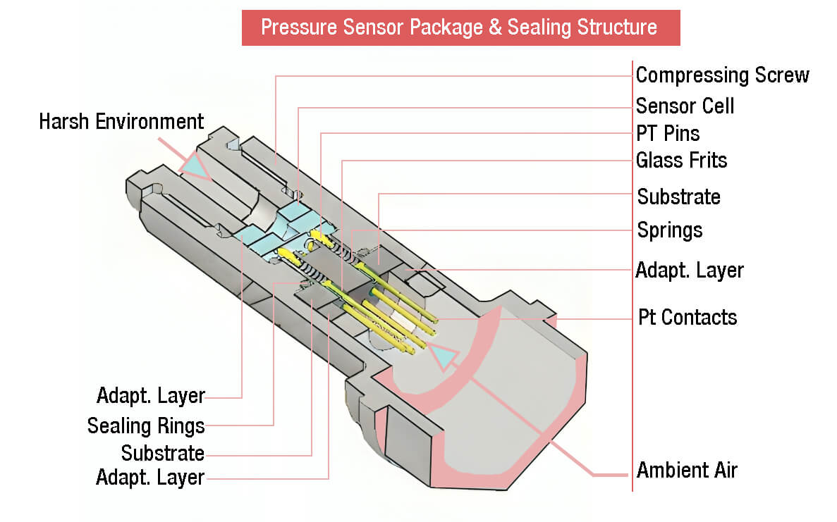
Hermetic packaging techniques, such as welding or brazing, are essential to prevent moisture ingress and ensure a leak-tight enclosure.
Materials used for packaging should have compatible CTEs with the sensor components to minimize stress and deformation at high temperatures. Glass-to-metal sealing or ceramic packaging may be employed for high-temperature applications.
Signal Conditioning and Interfacing
High-temperature signal conditioning circuits and interfacing components are required to ensure proper operation and accuracy at elevated temperatures.
Specialized high-temperature operational amplifiers, analog-to-digital converters (ADCs), and microcontrollers can be used to process and digitize the sensor output signals.

Digital signal processing techniques can further enhance accuracy, stability, and temperature compensation capabilities.
How to design High Accuracy thin film pressure sensor
To achieve high accuracy like 0.1% or 0.25% , the designers always need to focus on several key aspects of the sensor design and manufacturing process.
First, the diaphragm, which is the primary component responsible for translating the applied pressure into mechanical deflection, needs to be designed with utmost precision. The diaphragm thickness and geometry play a crucial role in determining the sensor’s sensitivity and linearity.
Typically, materials like silicon, silicon nitride, or single-crystal silicon carbide are used for high-accuracy diaphragms. The thickness can range from a few micrometers to tens of micrometers, depending on the pressure range and desired sensitivity.
Additionally, specialized diaphragm geometries, such as corrugated or bossed designs, can improve linearity and reduce stress concentrations, which can affect accuracy.
Next, the thin-film sensing element, which converts the diaphragm’s deflection into an electrical signal, must exhibit excellent piezoresistive properties, stability, and minimal hysteresis (the tendency to exhibit different output values for the same input, depending on the direction of change).
Sputtered or implanted polysilicon is a common choice due to its high sensitivity and good linearity. Silicon carbide thin films can also be used, especially in high-temperature applications, as they offer exceptional stability and linearity.
Effective temperature compensation is crucial for maintaining high accuracy over a wide temperature range. This involves integrating on-chip temperature sensors, such as resistive temperature detectors or diodes, and implementing advanced compensation algorithms in the signal conditioning circuitry or digital signal processing.
These algorithms can account for non-linear temperature effects, variations in material properties, and offset and span errors, ensuring accurate pressure measurements across the entire temperature range.
High-resolution analog-to-digital converters (ADCs) with low noise and high linearity are essential for achieving high accuracy.
Specialized instrumentation amplifiers with low offset and drift can be used to amplify the sensor’s output signals with minimal error.
Digital signal processing techniques, such as linearization algorithms, filtering, and advanced calibration methods, can further enhance accuracy and compensate for non-linearities and errors.
Rigorous calibration and trimming processes are necessary to achieve high accuracy specifications. Laser trimming techniques can be used to precisely adjust the resistor values in the sensing element or bridge circuit, minimizing offset and span errors.
Automated calibration systems and mathematical models can be employed to characterize and compensate for non-linearities, hysteresis, and other error sources.
Finally, hermetic packaging techniques, such as welding or brazing, are essential to prevent moisture ingress and ensure long-term stability. Packaging materials and designs should minimize stress concentrations and thermal gradients that can introduce errors or non-linearities.
Environmental protection measures, such as shielding and filtering, may also be necessary to minimize electromagnetic interference (EMI) and other external factors that can affect accuracy.
By carefully considering and optimizing these various aspects of the sensor design, manufacturing, and calibration processes, it is possible to achieve thin-film pressure sensors with high accuracy levels, such as 0.1% or 0.25% of the full-scale output.
Click to check more details about Pressure Sensor Accuracy
Other Piezo-Resistive Pressure Sensors
On top of above discussed Thin-film pressure sensor which using piezo-resistive principle, with four resistors are placed on a diaphragm in a Wheatstone bridge pattern to track the diaphragm’s deformation under pressure.
There are also other types of piezoresistive pressure sensor, like the following:
Ceramic Thick-Film Pressure Sensor
Thick-film sensors use the same setup as thin-film sensors by grouping four resistors into a Wheatstone bridge. But instead of attaching them to the base, thick-film sensors print the resistors onto a base such as ceramic using special technology, and then they heat it to a high temperature. They also detect change in resistance due to the diaphragm’s deformation, caused by stretching and compressing the material.
Diffused Silicone Piezo-resistive Pressure Sensor
Unlike the first two types, diffused silicone, actually act as kind of semi-conductor to uses a silicon measuring diaphragm with special diffused structures. They take advantage of the piezoresistive effect, which involves changing electrical resistance in the silicon due to stretching and compressing, thereby affecting electron mobility under mechanical stress.
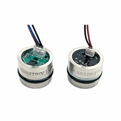
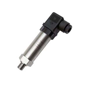
EST380 Thin-Film Pressure Sensor
Thin-Film | Silicon Carbide | Sputtered | Hermetic Packaging
0-4bar-2200bar | -40℃~150℃ | 0.1%.FS/0.25%/FS